Austrochip 2024
The Austrian Workshop on Microelectronics (Austrochip) is an annual meeting and platform
to present the latest activities in the field of micro- and nanoelectronic devices and
integrated circuits in Austria and neighboring countries.
The workshop is a forum for discussion and contact between academia and industry.
This 32nd edition of the Austrochip conference is jointly organized by the
Institute for Microelectronics
and the
Institute of Computer Engineering
at TU Wien.
The confernece and the associated workshops will take place on September 25-26, 2024 at TU Wien, Vienna, Austria.
News
- September 26, 2024: Best Paper Award Winners
- July 24, 2024: Registration Page
- July 01, 2024: Final Deadline Extension
- June 14, 2024: Submission Deadline Extension
- June 05, 2024: Submission Page
- March 14, 2024: Call for Papers
- February 27, 2024: New Sponsor
- February 14, 2024: New Sponsor
- February 13, 2024: New Sponsor
- February 08, 2024: New Sponsor
- February 05, 2024: New Sponsor
- February 05, 2024: New Sponsor
- January 31, 2024: New Sponsor
- January 30, 2024: New Sponsor
- January 25, 2024: New Sponsor
- January 24, 2024: New Sponsor
- January 23, 2024: New Sponsor
- January 22, 2024: New Sponsor
- October 26, 2023: Website Online
We congratulate Maximilian Ell, Ahmet Büyükakyüz and Günther Zeck for winning the Austrochip 2024 Best Paper Award.
Our ConfTool registration page in now online.
The final submission deadline is on July 8.
The paper submission deadline has been extended to July 1.
The Austrochip 2024 paper submission page is now online.
The Call for Papers is online. We are looking forward to many submissions!
We are pleased to announce our new Gold-level sponsor Intel.
We are pleased to announce our new Gold-level sponsor IMS Nanofabrication.
We are pleased to announce our new Silver-level sponsor F&S BONDTEC Semiconductor GmbH.
We are pleased to announce our new Bronze-level sponsor STMicroelectronics.
We are pleased to announce our new Gold-level sponsor SMT.
We are pleased to announce our new Gold-level sponsor ARTEMES.
We are pleased to announce our new Silver-level sponsor ams OSRAM.
We are pleased to announce our new Silver-level sponsor Beyond Gravity Austria GmbH.
We are pleased to announce our new Gold-level sponsor NXP Semiconductors.
We are pleased to announce our new Silver-level sponsor x.test GmbH.
We are pleased to announce our new Gold-level sponsor IPCEI Microelectronics and Communication Technologies.
We are pleased to announce our new Gold-level sponsor Infineon Technologies Austria AG.
The Austrochip 2024 Website is now online. A big thank you goes to last year's team for preparing a new responsive website template.
Important Dates
| Paper Submission Deadline |
08.07.2024 |
| Notification of Acceptance |
16.08.2024 |
| Tutorials/Workshops |
25.09.2024 |
| Conference |
26.09.2024 |
| Registration |
22.09.2024 |
Call for Papers
For the Austrochip 2024 conference authors are requested to submit an extended abstract, inclusive of representative data and figures, describing the outcomes of their research endeavors and stating their significance.
Topics
Topics of the workshop include but are not limited to
- Micro- and Nanoelectronic Devices
- Simulation of microelectronics devices and processes (TCAD)
- Device reliability characterization and analysis (Noise/RTN, BTI, SILC, TDDB)
- Robustness of power and wide bandgap devices and circuits (SiC, GaN, etc.)
- Emerging technologies and devices (SiGe, 2D materials, etc.)
- Reliability tests for monitoring and qualification (wafer-level, package-level, etc.)
- Device to circuit degradation
- Integrated Circuits
- Analog, mixed-signal, and RF integrated circuits
- Digital circuits, filters, DSPs, asynchronous designs
- FPGA design and reconfigurable hardware
- Design methodology, system-level design, giga scale circuits, network-on-chip
- Embedded systems and IoT, energy-efficient machine learning, low-power designs, RF systems, security aspects
- Verification and testing, signal integrity, compact device modeling, timing analysis, reliability simulation, EMC, ESD, radiation effects
- Quantum computing, sub-threshold circuits, sensors, organic and biomedical electronics
- Case studies and prototyping
Review Process and Proceedings
All submissions go through a double-blind review process and have to fulfill the requirements of IEEE Xplore. The accepted papers will be chosen for either oral or poster presentation based on their merit. All accepted papers will be published in IEEE explore after the conference. The committee strongly encourages contributions from both academic and industrial domains.
Submission
Please submit your contributions via our ConfTool submission system.
Submission Guidelines
- Format has to be in A4 format according to the IEEE style.
- Anonymous - remove authors, institutions, and the acknowledgment as papers will be double-blind reviewed.
- Papers should not exceed 4 pages (including bibliography and appendix).
- Papers must be written in English and submitted in PDF file format.
- Original, unpublished work - not simultaneously submitted to other workshops, conferences, or journals.
Papers not meeting these guidelines risk rejection without consideration! Austrochip 2024 reserves the right to exclude any accepted paper from distribution after the conference if the accepted paper is not presented at the conference. This means that every accepted paper needs at least one full registration for the conference.
Special Issue in Microelectronics Engineering Journal
Up to ten papers will be invited to submit an extended version of their work to the special issue Advances in Micro- and Nanoelectronic Devices and Circuit Engineering published in the Microelectronics Engineering Journal. The submission deadline for the extended papers is January 31, 2025.
Registration
Registration for the conference via our ConfTool system is now open. Please note that each accepted paper, requires one full conference registration!Conference Packages
You have the option to attend to full Austrochip 2024 conference event, or just either of the two days.
| Package | Contents | ||
| Full Conference | tutorials and technical sessions, coffee breaks and lunch break, gala dinner | ||
| Tutorial day | tutorials on September 25th, coffee breaks | ||
| Main conference day | technical sessions on September 26th, coffee breaks and lunch break | ||
| Additional gala dinner | an additional ticket for the gala dinner on September 25th |
| Package | Regular Fee | Late Fee | Master Students |
| Full conference | 220 € | 240 € | -- |
| Tutorial day | 75 € | 80 € | FREE! |
| Main conference day | 145 € | 160 € | FREE! |
| Additional gala dinner | 90 € | 100 € | -- |
Keynotes
Keynote 1: Semiconductor Reliability: Future Trends, Challenges, and Opportunities
Abstract
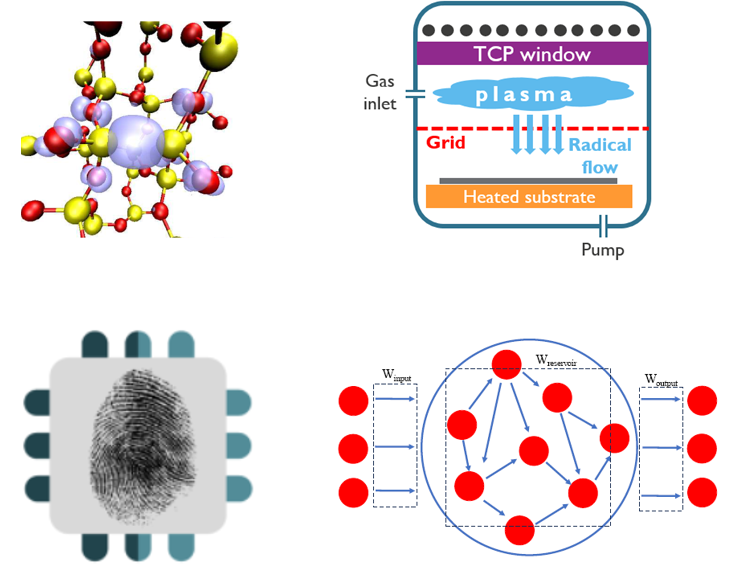
The presence of non-idealities and defects in VLSI technologies is an immutable reality, which, however, is often overlooked by device engineers, researchers, technologists, and designers alike. I will argue that VLSI reliability, in fact, “makes or breaks” any new technology. Superficial device reliability optimization is possible using phenomenological observations only, but I will argue that solid physical foundations and a thorough understanding of the underlying degradation mechanisms are essential both for truly dependable lifetime projections and for novel device pathfinding. Based on the detailed investigation of gate oxide defects, our “defect engineering” approach enables, among other things, oxidation techniques for advanced VLSI architectures. In deeply scaled devices, degradation mechanisms can be decomposed down to individual defects, with each defect measured separately. Such knowledge then allows us, e.g., to model the degradation statistics of deeply-scaled devices and to predict the likelihood of their failure. Robust degradation models enable us to project wider safe operating areas, which in turn allow us to design better-performing circuitry at a given technology node and thus limit costs. Moreover, the ubiquitous presence of defects can be, in fact, embraced, and the in-depth knowledge of defect properties can be used to our advantage to design new devices and applications, ranging from tamper-aware chip ageing monitors to physically unclonable functions and reservoir computing to identify users.
About Ben Kaczer
Dr. Ben Kaczer is a Scientific Director in the FEOL reliability group (DRE) at imec. Dr. Kaczer received the M.S. degree in Physical Electronics from Charles University, Prague, in 1992 and the M.S. and Ph.D. degrees in Physics from The Ohio State University, in 1996 and 1998, respectively. In 1998 he joined the reliability group of imec, Leuven, Belgium, where his activities have included the research of the degradation phenomena and reliability assessment of SiO2, SiON, high-k, and ferroelectric films, planar and multiple-gate FETs, circuits, and characterization of Ge, SiGe, III-V, MIM, and TMD devices.
He has co-authored more than 600 journal and conference papers and 4 patent groups related to device and circuit reliability, presented a number of invited papers and tutorials, and received and co-received 6 IEEE International Reliability Physics Symposium (IRPS) Best and Outstanding Paper Awards, 2 IEEE IPFA Best Paper Awards, and the 2011 IEEE EDS Paul Rappaport Award.
Dr. Kaczer has served twice as the chair of the Characterization, Reliability and Yield subcommittee of the International Electron Device Meeting (IEDM; 2007 and 2015) and as a member of various subcommittees of the IRPS (2002—2016) and is currently serving as a member of IRPS management committee (2018—). He was the General Chair of the Semiconductor Interfaces Specialists Conference (SISC; 2006) and continues to act as the conference secretary (2007—). He co-organized the INFOS conference (2005), and served on the INFOS, WoDiM, IPFA, and ICICDT conference committees. He has served on the Editorial Board of IEEE Journal of Transaction of Electron Devices for three terms (2011—2019).
Keynote 2: 2D Materials for Quantum Space Applications
Abstract
Modern (asymmetric) encryptions are based on unproven mathematical assumptions such as the complexity of the factorization problem. Quantum computers will be able to efficiently break these encryptions, making internet connections insecure. One of the replacement candidates is quantum key distribution (QKD), where the information is encoded in single photon states of light. Due to the fundamental laws of quantum physics, any eavesdropping attempt would be immediately revealed.
For QKD to work in the field, one needs to generate single photons and transmit them over long distances. In this talk, I will present our efforts in realizing a compact room temperature single photon source based on a color center in the 2D material hexagonal boron nitride. The performance is sufficient to outperform laser-based QKD protocols. The emitter is directly coupled to a photonic integrated circuit that routes the single photons to different experiments. The payload is currently being integrated on a 3U CubeSat and will be launched in 2025 as part of the QUICK3 mission. A constellation of small satellites equipped with the technology developed in QUICK3 could serve as a backbone for a satellite-based quantum internet. Moreover, 2D materials can also be used to build radiation-tolerant and ultra-low weight electronics or opto-electronics and have been qualified by us for use on satellites.
Figure Caption: Performance of 2D material-based devices for space applications. (a) Simulation of the radiation environment in LEO at 500 km altitude. Licensed under CC BY 4.0 (Ref. [1]) (b) Quantum emitter array in hexagonal boron nitride (hBN) for satellite-based quantum communication. Reprinted (adapted) with permission (Ref. [2]). Copyright 2024, American Chemical Society. (c) Atomically-thin field-effect transistor (FET) for light-weight satellite electronics. Licensed under CC BY 4.0 (Ref. [1]) (d) Performance of the hBN emitter for space-to-ground scenarios in daylight conditions (red dots). Licensed under CC BY 4.0 (Ref. [3]) (e) Performance of the 2D-FET before and after space qualification. Licensed under CC BY 4.0 (Ref. [1]).
[1] Nat. Commun. 10, 1202 (2019)
[2] ACS Nano 18, 5270-5281 (2024)
[3] APL Quantum 1, 016113 (2024)
About Tobias Vogl
Tobias Vogl studied physics at the University of Munich. For the PhD he moved to the Australian National University, where he developed processes around quantum emitters in the 2D material hexagonal boron nitride. These quantum emitters were further advanced and brought into applications during postdoc positions at the University of Cambridge and the University of Jena. In 2022 he started his own junior research group at the University of Jena and was shortly afterwards appointed as one of the youngest permanent Professors in Germany at the Technical University of Munich. He is also the coordinator of the QUICK3 space mission and received several research prizes.
Tutorials
Tutorial 1: Semiconductor Fabrication at Multiple Time and Length Scales
Abstract
The microelectronics industry has undergone significant innovation in recent years. The decades-long technology roadmap that involved planar transistor scaling has nowadays evolved into a search for optimal geometries and materials beyond silicon. With this change, circuit designers and fabrication engineers can no longer enjoy the benefits of decades of experimental information on silicon. Technology computer-aided design (TCAD) and design-technology co-optimization (DTCO) strategies need to adapt to include the search for novel materials through a multi-scale modeling approach, where the atomistic behavior of a material informs design decisions. Furthermore, with a continued reduction of design margins, process variability is becoming a significant concern. Understanding equipment-level and across-wafer variation is paramount. However, current implementations of physical deposition and etching models do not provide a direct link to equipment inputs.
This talk will discuss the current state of process simulation and emulation, and what we are currently investigating and developing to assist the microelectronics industry, which includes both semiconductor manufacturers and electronic design automation (EDA) vendors. In this tutorial, we will cover several aspects essential to modeling semiconductor fabrication. The inclusion of TCAD and DTCO during the design process has become invaluable and for these, both time-discretized physical models and quick geometric emulations have a role to play. The tutorial will also discuss how machine learning is helping merge feature-scale modeling approaches with reactor-level inputs and equipment variability. The applied method can provide semiconductor manufacturers a virtual copy of their equipment, which is directly linked to physical and empirical deposition and etching models. Ultimately, this creates a pathway towards a digital DTCO strategy for design discovery while reducing cost, time, and the environmental impact of a design cycle by reducing the heavy reliance on experimental wafer fabrication.

About Lado Filipovic
Lado Filipovic is an Associate Professor and the Director of the Christian Doppler Laboratory for Multi-Scale Process Modeling of Semiconductor Devices and Sensors at the Institute for Microelectronics, TU Wien. Lado’s research is centered around Integrated Semiconductor Sensors, Process Technology Computer Aided Design (TCAD), and the integration of artificial intelligence in TCAD. He obtained his venia docendi (habilitation) in Semiconductor Based Integrated Sensors and his doctoral degree (Dr.techn.) in Microelectronics from TU Wien in 2020 and 2012, respectively. Lado is currently heading several research projects at a wide range of technology readiness levels (TRLs) from basic research to industry applications. His research team has released several open-source scientific software tools under the ViennaTools moniker, such as the process simulator ViennaPS which is currently used for studying the fabrication of advanced nanoelectronic devices in academia and industry worldwide.
Tutorial 2: Cryogenic CMOS Technologies for Quantum Computing Systems
Abstract
Large-scale quantum computers are not only contenders to break limits of CMOS computing but also have the potential to massively boost fundamental research in fields such as cryptography, computational chemistry, and material science. Integrating CMOS circuits and qubits at cryogenic temperatures is one of the key challenges to mitigate wiring constraints and ensure signal integrity to enable up-scaling of quantum computers. Interfaces between classical and quantum circuits need to maintain ultra-low power consumption together with very low noise figures, therefore it is necessary to develop on-chip solutions with ultra-low power consumption and optimized (noise-) performance. Lowering the supply voltage for cryogenic circuits is the most common approach to lower power consumption, hence the margins for device reliability and variability of CMOS devices at cryogenic temperatures is a topic of great interest.
In this tutorial we will cover aspects of device performance, device-to-device variability and parameter degradation of transistors at cryogenic temperatures. Additionally, the temperature scaling of low-frequency noise and the role of band-tails, as well as models for charge trapping kinetics at cryogenic temperatures will be discussed. We will also give some application examples for integrated cryo-CMOS circuits designed to overcome the measurement bottleneck arising in most cryogenic probers.
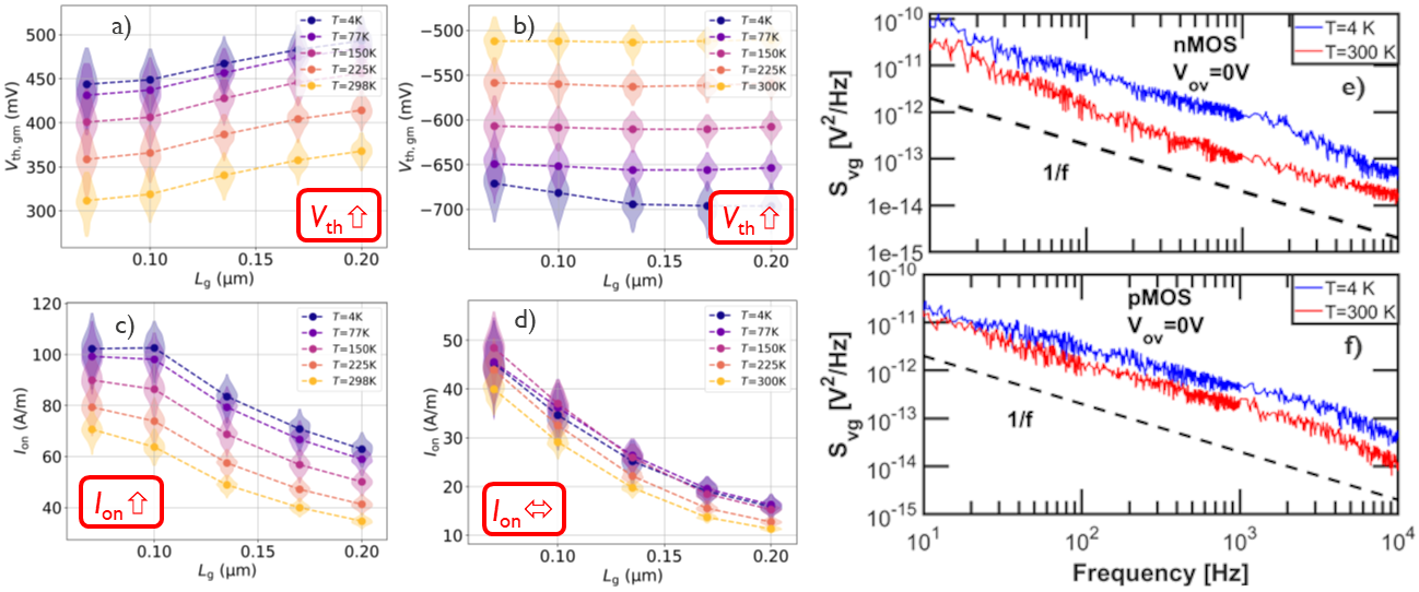
Figure Caption: Parameter distributions of Vth and Ion as function of temperature and gate length for a large set of nMOS (a,c) and pMOS (b,d) 28nm bulk CMOS devices. The scaling of the average values is illustrated in the red boxes. Panels e and f show a significant increase of low-frequency with lower temperature, commonly attributed to the role of band-tails.
About Alexander Grill
Alexander Grill studied Microelectronics at TU Vienna, where he received his master’s degree in 2013 and his doctoral degree in 2018. He is currently working as a principle researcher for cryogenic CMOS electronics at imec, Leuven. His main scientific interests are characterization and modeling of semiconductor devices at cryogenic temperatures with a special focus on charge trapping, charge noise, and reliability. His current focus is studying time-zero variability and device degradation to enable the design of low-noise, low-power circuits at cryogenic temperatures down to the mK regime. He has authored and coauthored more than 80 journal articles and conference contributions. Additionally, he is principle investigator of the European project ARCTIC, which brings together 36 institutions from Europe and Canada to push forward materials, circuits, and applications for cryogenic CMOS electronics.
Tutorial 3: Radiation Effects in Integrated Circuits
Abstract
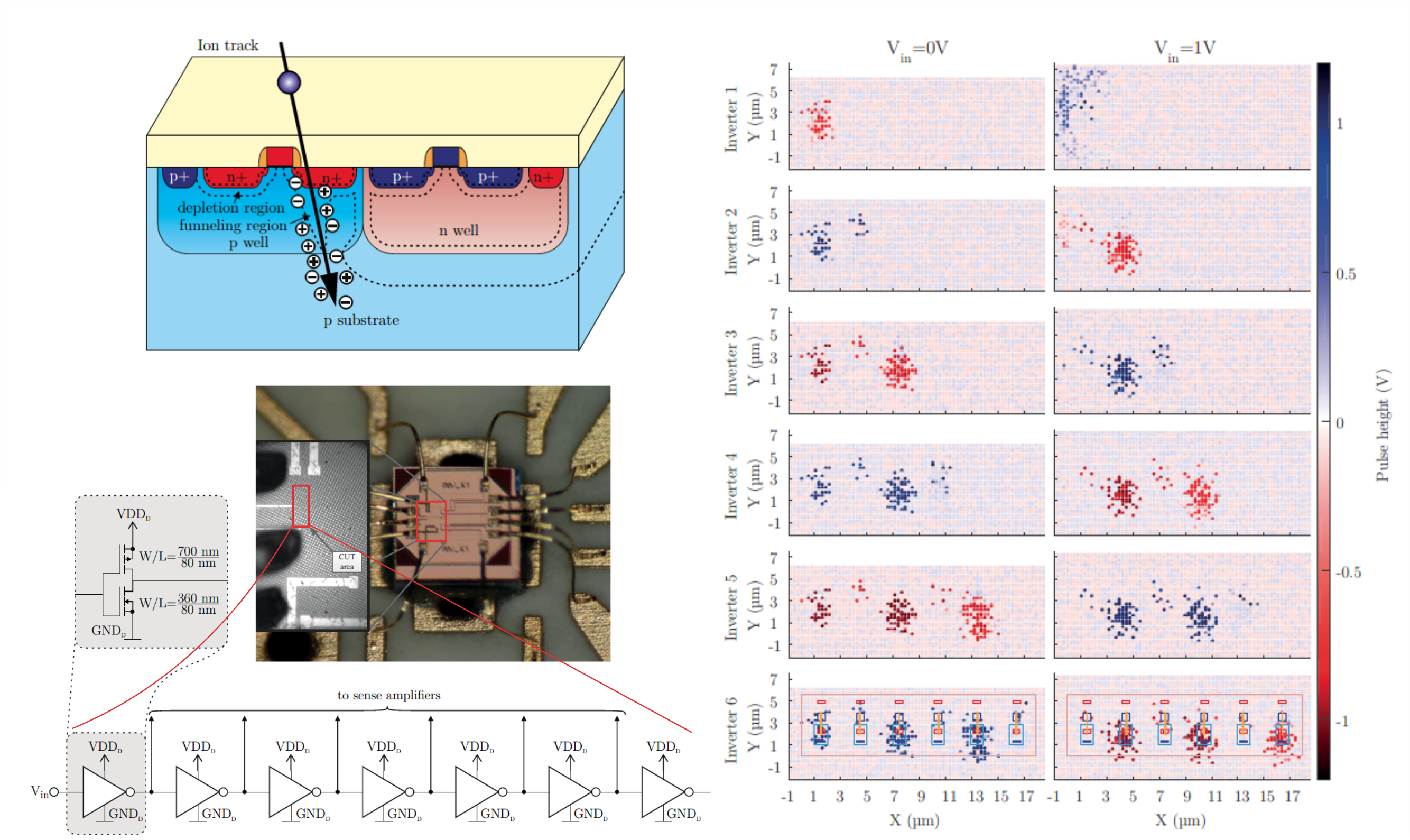
Especially for aerospace applications, radiation effects are a crucial factor that can cause destructive and non-destructive failures, which can have catastrophic effects. The continuous reduction in the critical dimensions of devices also leads to a steadily decreased amount of critical charge sufficient to cause a single event effect. Consequently, radiation effects could also become important for ground applications. The investigation of such radiation effects is therefore of crucial importance for the reliability of integrated circuits.
In this tutorial, we will discuss the main sources of radiation that cause these effects. Furthermore, we will cover the basic mechanisms of radiation effects, including single-evet effects that can be divided into soft errors, which can result in unexpected behavior of a circuit or a system, and hard errors, which typically lead to permanent errors, as well as total dose effects, which lead to a degradation of devices depending on the received radiation dose. We will also discuss how scaling trends and different technology types (such as bulk CMOS and SOI) affect the vulnerability of the integrated circuits. Finally, we will look at methods to study these radiation effects, with a focus on position resolving approaches that allow identifying the vulnerable regions of an integrated circuit.
About Michael Hofbauer

Michael Hofbauer received the Dipl.-Ing. degree in electrical engineering, and the Ph.D. degree (Hons.) sub auspiciis praesidentis from TU Wien, Vienna, Austria, in 2011 and 2017, respectively. Since 2005, he has been as student worker and project assistant with the Institute of Electrodynamics Microwave and Circuit Engineering, TU Wien, where he became a University Assistant in 2016. His research interests are in the investigation of radiation effects in electronics, electronic-photonic integration, and optical metrology. He has authored and coauthored more than 80 journal articles and conference contributions. Additionally, he has contributed to many national and international (EU) projects. Among other projects, he has recently finished his own FWF standalone project and is currently co-heading another one.
Tutorial 4: Open-Source Design of Integrated Circuits
Abstract
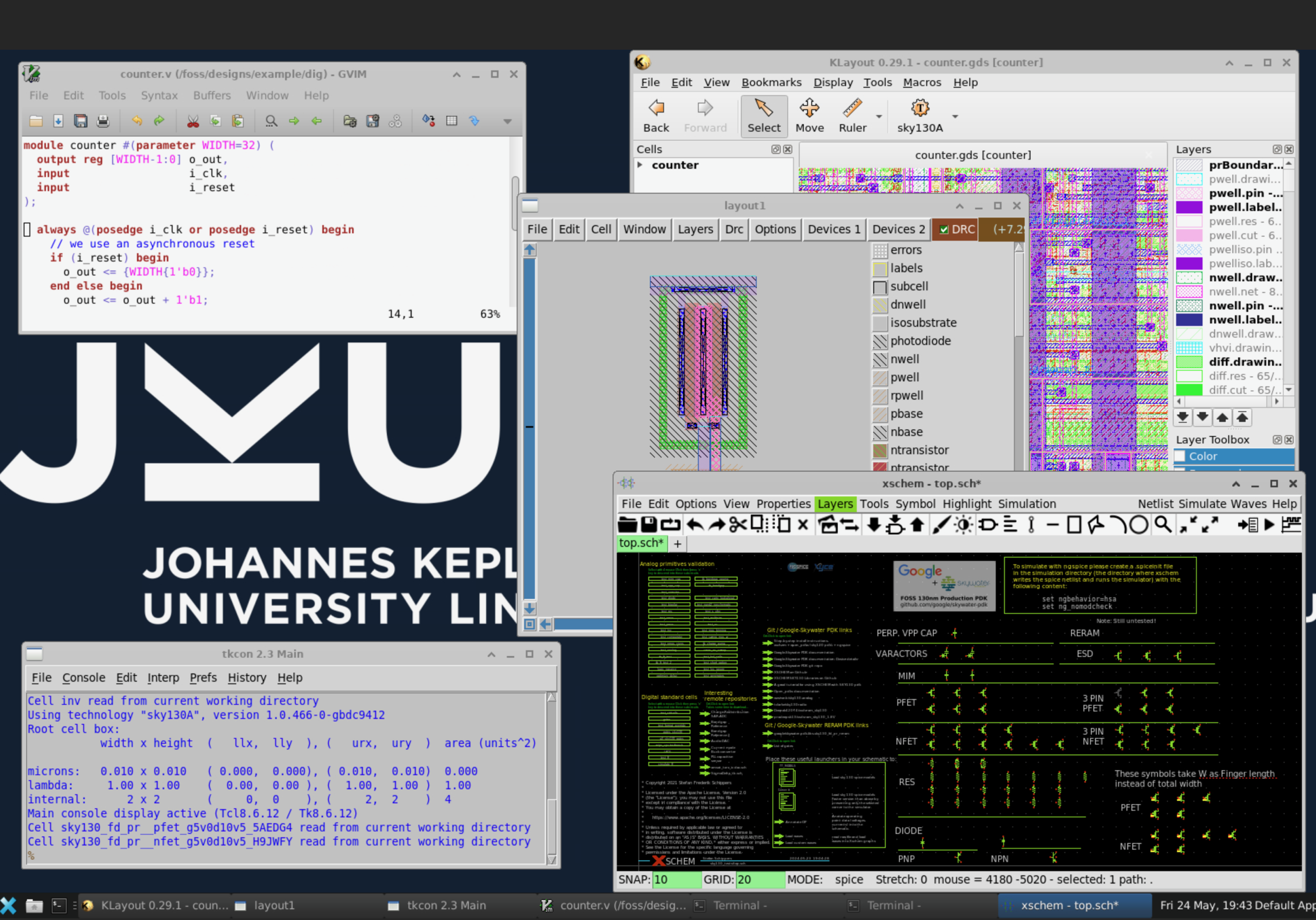
During this hands-on tutorial, we will examine the driving factors behind the growing popularity of open-source integrated circuit (IC) design tools. Additionally, we will explore the current state of these tools and the recently introduced open-source process design kits. We will present a meticulously selected collection of electronic design automation (EDA) tools and discuss their utilization in a mixed-signal circuit design flow. Furthermore, we will highlight recent advancements that have been made possible through the collaborative nature of open-source projects. A few live, interactive demos will be performed (analog schematics and layout, DRC, LVS, PEX, digital RTL2GDS), and everyone who brings a notebook with access to the internet and a browser will be able to follow along using a provided virtual EDA machine.
About Harald Pretl
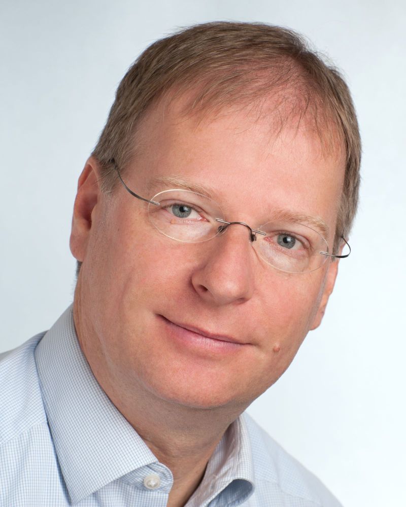
Harald Pretl received a Dipl.-Ing. degree (with distinction) in electrical engineering from the Graz University of Technology, Austria, in 1997, and the Dr. techn. degree from the Johannes Kepler University (JKU) in Linz, Austria, in 2001. From 2000 to 2011, he worked at Infineon Technologies as Director and Senior Principal Engineer, from 2011 to 2019 at Intel as Senior Principal Engineer and Chief RF Technologist, and from 2019 to 2022 at Apple, contributing to several generations of cellular RF transceivers. Since 2015, he has been a full professor, heading the Institute for Integrated Circuits (IIC) at JKU. He maintains the IIC-OSIC-TOOLS and is a member of the IEEE SSCS TC-OSE. He is currently a visiting researcher at IHP Microelectronics. In 2023, Harald founded PRETL consult GmbH, providing consulting services in the area of IC design.
Committees
Organizing Committee
| Michael Waltl | General Chair |
| Florian Huemer | General Chair |
| Michael Hofbauer | Technical Program Chair |
| Diana Pop | Organization and Management |
Technical Program Committee
Steering Committee
| Mario Huemer | click to reveal email address |
| Michael Hutter | click to reveal email address |
| Timm Ostermann | click to reveal email address |
| Peter Rössler | click to reveal email address |
| Kerstin Schneider-Hornstein | click to reveal email address |
| Andreas Steininger | click to reveal email address |
| Johannes Sturm | click to reveal email address |
| Peter Söser | click to reveal email address |
Venue
Austrochip 2024 will be held at Campus Gußhaus at TU Wien. Both the conference and the workshop will take place in the EI 10 Fritz Paschke lecture hall, Gusshausstrasse 27-29, 1040 Wien.
Travel and Transportation
By Public Transport
The Campus Gußhaus is not far away from the central railway station of Vienna. From there you can take the U1 metro line in the direction of Floridsdorf for one station and exit at Taubstummengasse. It is also possible to walk, which will take approximately 20 minutes.
By Car
There are several parking garages in the vicinity of conference venue, one being directly next to the building.
Possible Hotels
| Schick Hotel Erzherzog Rainer |
| Hotel Johann Strauss |
| Austria Trend Hotel beim Theresianum |
| Hotel Motel One Wien-Hauptbahnhof |
| Novotel Wien Hauptbahnhof |
Sponsors
This section is dedicated to the companies and organisations that are generously supporting Austrochip 2024. These sponsors are instrumental in making our event possible and a major factor in its success.Gold
ARTEMES

IMS Nanofabrication

Infineon Technologies Austria AG

Intel

IPCEI Microelectronics and Communication Technologies

NXP Semiconductors
SMT

Silver
ams OSRAM

Beyond Gravity Austria GmbH

F&S BONDTEC Semiconductor GmbH

x.test GmbH

Bronze
STMicroelectronics
Technical
IEEE Austria Section
