Tutorials
We are pleased to announce that Austrochip 2024 will feature four tutorials, which will take place on September 25. Thanks a lot to our speakers for sharing their insights and expertise with our audience.
- Semiconductor Fabrication at Multiple Time and Length Scales by Lado Filipovic
- Cryogenic CMOS Technologies for Quantum Computing Systems by Alexander Grill
- Radiation Effects in Integrated Circuits by Michael Hofbauer
- Open-Source Design of Integrated Circuits by Harald Pretl
Tutorial 1
Semiconductor Fabrication at Multiple Time and Length Scales
The microelectronics industry has undergone significant innovation in recent years. The decades-long technology roadmap that involved planar transistor scaling has nowadays evolved into a search for optimal geometries and materials beyond silicon. With this change, circuit designers and fabrication engineers can no longer enjoy the benefits of decades of experimental information on silicon. Technology computer-aided design (TCAD) and design-technology co-optimization (DTCO) strategies need to adapt to include the search for novel materials through a multi-scale modeling approach, where the atomistic behavior of a material informs design decisions. Furthermore, with a continued reduction of design margins, process variability is becoming a significant concern. Understanding equipment-level and across-wafer variation is paramount. However, current implementations of physical deposition and etching models do not provide a direct link to equipment inputs.
This talk will discuss the current state of process simulation and emulation, and what we are currently investigating and developing to assist the microelectronics industry, which includes both semiconductor manufacturers and electronic design automation (EDA) vendors. In this tutorial, we will cover several aspects essential to modeling semiconductor fabrication. The inclusion of TCAD and DTCO during the design process has become invaluable and for these, both time-discretized physical models and quick geometric emulations have a role to play. The tutorial will also discuss how machine learning is helping merge feature-scale modeling approaches with reactor-level inputs and equipment variability. The applied method can provide semiconductor manufacturers a virtual copy of their equipment, which is directly linked to physical and empirical deposition and etching models. Ultimately, this creates a pathway towards a digital DTCO strategy for design discovery while reducing cost, time, and the environmental impact of a design cycle by reducing the heavy reliance on experimental wafer fabrication.

About Lado Filipovic
Lado Filipovic is an Associate Professor and the Director of the Christian Doppler Laboratory for Multi-Scale Process Modeling of Semiconductor Devices and Sensors at the Institute for Microelectronics, TU Wien. Lado’s research is centered around Integrated Semiconductor Sensors, Process Technology Computer Aided Design (TCAD), and the integration of artificial intelligence in TCAD. He obtained his venia docendi (habilitation) in Semiconductor Based Integrated Sensors and his doctoral degree (Dr.techn.) in Microelectronics from TU Wien in 2020 and 2012, respectively. Lado is currently heading several research projects at a wide range of technology readiness levels (TRLs) from basic research to industry applications. His research team has released several open-source scientific software tools under the ViennaTools moniker, such as the process simulator ViennaPS which is currently used for studying the fabrication of advanced nanoelectronic devices in academia and industry worldwide.
Tutorial 2
Cryogenic CMOS Technologies for Quantum Computing Systems
Large-scale quantum computers are not only contenders to break limits of CMOS computing but also have the potential to massively boost fundamental research in fields such as cryptography, computational chemistry, and material science. Integrating CMOS circuits and qubits at cryogenic temperatures is one of the key challenges to mitigate wiring constraints and ensure signal integrity to enable up-scaling of quantum computers. Interfaces between classical and quantum circuits need to maintain ultra-low power consumption together with very low noise figures, therefore it is necessary to develop on-chip solutions with ultra-low power consumption and optimized (noise-) performance. Lowering the supply voltage for cryogenic circuits is the most common approach to lower power consumption, hence the margins for device reliability and variability of CMOS devices at cryogenic temperatures is a topic of great interest.
In this tutorial we will cover aspects of device performance, device-to-device variability and parameter degradation of transistors at cryogenic temperatures. Additionally, the temperature scaling of low-frequency noise and the role of band-tails, as well as models for charge trapping kinetics at cryogenic temperatures will be discussed. We will also give some application examples for integrated cryo-CMOS circuits designed to overcome the measurement bottleneck arising in most cryogenic probers.
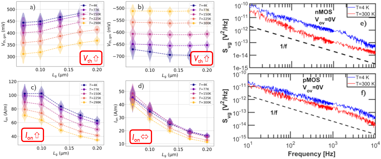
Parameter distributions of Vth and Ion as function of temperature and gate length for a large set of nMOS (a,c) and pMOS (b,d) 28nm bulk CMOS devices. The scaling of the average values is illustrated in the red boxes. Panels e and f show a significant increase of low-frequency with lower temperature, commonly attributed to the role of band-tails.
About Alexander Grill
Alexander Grill studied Microelectronics at TU Vienna, where he received his master’s degree in 2013 and his doctoral degree in 2018. He is currently working as a principle researcher for cryogenic CMOS electronics at imec, Leuven. His main scientific interests are characterization and modeling of semiconductor devices at cryogenic temperatures with a special focus on charge trapping, charge noise, and reliability. His current focus is studying time-zero variability and device degradation to enable the design of low-noise, low-power circuits at cryogenic temperatures down to the mK regime. He has authored and coauthored more than 80 journal articles and conference contributions. Additionally, he is principle investigator of the European project ARCTIC, which brings together 36 institutions from Europe and Canada to push forward materials, circuits, and applications for cryogenic CMOS electronics.
Tutorial 3
Radiation Effects in Integrated Circuits
Especially for aerospace applications, radiation effects are a crucial factor that can cause destructive and non-destructive failures, which can have catastrophic effects. The continuous reduction in the critical dimensions of devices also leads to a steadily decreased amount of critical charge sufficient to cause a single event effect. Consequently, radiation effects could also become important for ground applications. The investigation of such radiation effects is therefore of crucial importance for the reliability of integrated circuits.
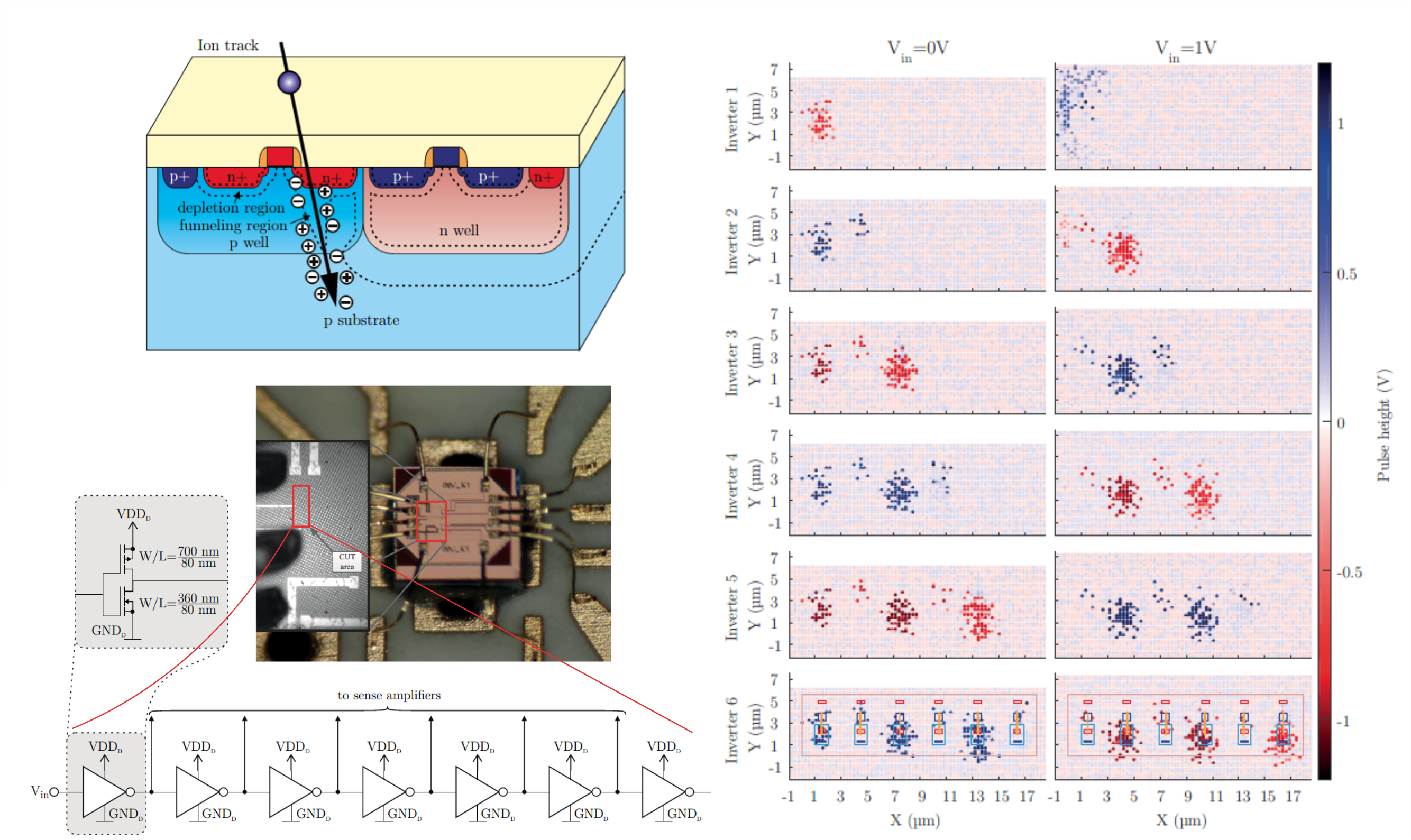
In this tutorial, we will discuss the main sources of radiation that cause these effects. Furthermore, we will cover the basic mechanisms of radiation effects, including single-evet effects that can be divided into soft errors, which can result in unexpected behavior of a circuit or a system, and hard errors, which typically lead to permanent errors, as well as total dose effects, which lead to a degradation of devices depending on the received radiation dose. We will also discuss how scaling trends and different technology types (such as bulk CMOS and SOI) affect the vulnerability of the integrated circuits. Finally, we will look at methods to study these radiation effects, with a focus on position resolving approaches that allow identifying the vulnerable regions of an integrated circuit.
About Michael Hofbauer
Michael Hofbauer received the Dipl.-Ing. degree in electrical engineering, and the Ph.D. degree (Hons.) sub auspiciis praesidentis from TU Wien, Vienna, Austria, in 2011 and 2017, respectively. Since 2005, he has been as student worker and project assistant with the Institute of Electrodynamics Microwave and Circuit Engineering, TU Wien, where he became a University Assistant in 2016. His research interests are in the investigation of radiation effects in electronics, electronic-photonic integration, and optical metrology. He has authored and coauthored more than 80 journal articles and conference contributions. Additionally, he has contributed to many national and international (EU) projects. Among other projects, he has recently finished his own FWF standalone project and is currently co-heading another one.

Tutorial 4
Open-Source Design of Integrated Circuits
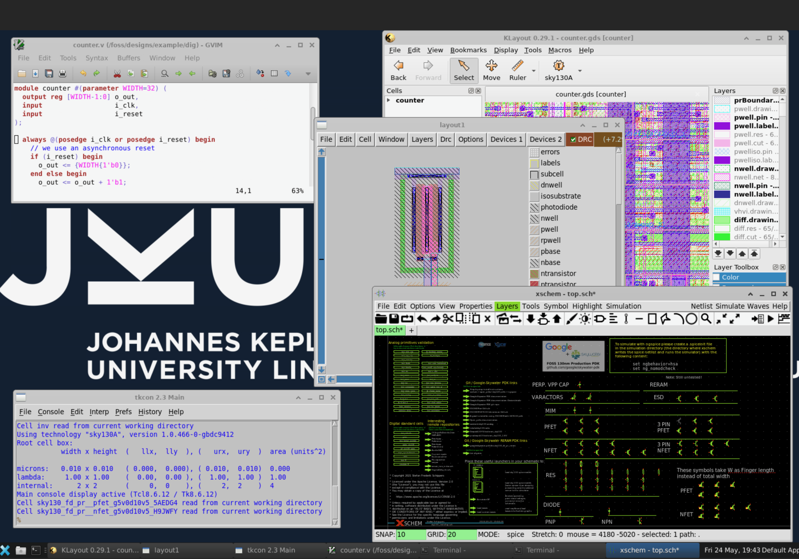
During this hands-on tutorial, we will examine the driving factors behind the growing popularity of open-source integrated circuit (IC) design tools. Additionally, we will explore the current state of these tools and the recently introduced open-source process design kits. We will present a meticulously selected collection of electronic design automation (EDA) tools and discuss their utilization in a mixed-signal circuit design flow. Furthermore, we will highlight recent advancements that have been made possible through the collaborative nature of open-source projects. A few live, interactive demos will be performed (analog schematics and layout, DRC, LVS, PEX, digital RTL2GDS), and everyone who brings a notebook with access to the internet and a browser will be able to follow along using a provided virtual EDA machine.
About Harald Pretl
Harald Pretl received a Dipl.-Ing. degree (with distinction) in electrical engineering from the Graz University of Technology, Austria, in 1997, and the Dr. techn. degree from the Johannes Kepler University (JKU) in Linz, Austria, in 2001. From 2000 to 2011, he worked at Infineon Technologies as Director and Senior Principal Engineer, from 2011 to 2019 at Intel as Senior Principal Engineer and Chief RF Technologist, and from 2019 to 2022 at Apple, contributing to several generations of cellular RF transceivers. Since 2015, he has been a full professor, heading the Institute for Integrated Circuits (IIC) at JKU. He maintains the IIC-OSIC-TOOLS and is a member of the IEEE SSCS TC-OSE. He is currently a visiting researcher at IHP Microelectronics. In 2023, Harald founded PRETL consult GmbH, providing consulting services in the area of IC design.
